
Solving yesterday's problems today
© 1999-2023 Jürgen Müller
juergen@e-basteln.de
Solving yesterday's problems today
© 1999-2023 Jürgen Müller
juergen@e-basteln.de
The general idea of the 65F02 is straightforward: Load all ROM content from the host computer into on-chip RAM upon startup, then execute everything from on-chip RAM at 100 MHz – except for memory-mapped I/O access, which goes to the external host bus at the original slow speed. But there are a few twists which the 65F02 needs to be aware of. Here’s what I have implemented (but not fully tested) so far, with thanks to the clever folks at 6502.org who came up with some of these ideas:
It was common practice in the days of the 6502 to use exactly timed code sequences to generate the timing required by some peripheral devices. The Apple II takes this to the extreme, relying on cycle-counted software loops to read its game controller “paddles”, control modulation and demodulation of data for the cassette recorder (the original data storage device), and even time data bits for the Disk II floppy drive. But most 6502 systems use timed code to some extent, e.g. to control the pitch of speaker sounds.
The 65F02 tries to get this right automatically, by falling back to the original host speed whenever it encounters an access to a memory address which is known to control “time critical” peripherals. This real time mode continues until the current code segment is left “upwards”, via an RTS or an RTI instruction. (Diving deeper into subroutines via additional JSR/RTS pairs is allowed of course, and does not terminate real time mode yet.) There is also a timeout mechanism, which switches back into fast mode after one second without any access to critical peripherals. This deals with initialization of peripherals from a program’s top level, for example.
This scheme is not bullet-proof. One can easily describe code patterns which either let the slow real time mode persist forever, or let the 65F02 switch back to fast clocking too early. But in practice it works well in many chess computers now, and in the Apple II it lets me boot and operate Apple DOS nicely.
In the larger microcomputers, text and graphics are displayed by writing data into special areas of the host’s RAM. This video RAM is also read in the background by a video display logic, which converts the contents into video signals to be displayed on a cathode ray tube. Obviously, the 65F02 must write video information to the slow, original host RAM; otherwise the data would never reach the display.
But the processor also needs to read the video RAM regularly – e.g. to scroll text on the screen, or to draw a line graphic on top of already existing lines. Do the reads have to be slow as well? The 65F02 makes sure that all write accesses to video RAM go to both, its on-chip RAM and the host RAM. Then a read access to video RAM will find the required information in the on-chip RAM, and can hence proceed at the full 100 MHz clock rate.
This feature is now implemented for the Apple II and the CBM/PET series. One benchmark where it really shines is “Brian’s Theme”, a graphics demo that shipped with the Apple, programmed by Brian Howard. It would draw sets of closely spaced radial lines from a random center point. The Apple’s limited graphics resolution translated into nice moiré effects. It looked like this (not my video):
I timed 20 repeats of Brian’s plots on my Apple II plus:
Original 1 MHz speed: 390 seconds
100 MHz, reading and writing the video RAM externally: 16.5 seconds
100 MHz, mirrored video RAM so reads are fast: 7 seconds
The 65F02 board provides standard JTAG signals which can be used to program and debug the FPGA, and to program the attached flash ROM for permanent storage of the FPGA configuration. But this requires a dedicated programming adapter from Xilinx (or a cheaper, but still special clone), as well as unwieldy PC-based programming software from Xilinx.
Luke Valenty to the rescue, who has developed a USB programming solution for his TinyFPGA series of FPGA boards. It consists of a USB/SPI bridge, which gets pre-installed in the FPGA, and the TinyProg Python program, which talks to it from any Windows/Linux/Mac computer. To make this solution robust and comfortable, Luke has designed it around a dual-boot FPGA configuration: The bootloader remains safe in a separate FPGA configuration image while a new user image is uploaded. Metadata residing in the flash ROM describe where the bootloader and the user image go, so TinyProg can handle this automatically.
Starting with board revision D, the 65F02 is compatible with Luke’s TinyProg, via a simple adapter board into which the 65F02 can be plugged. The USB/SPI bootloader is pre-installed in the 65F02’s flash ROM; the Python program can be downloaded from the official online repository. See the Files & Links page for details and for information on the open-source licenses.
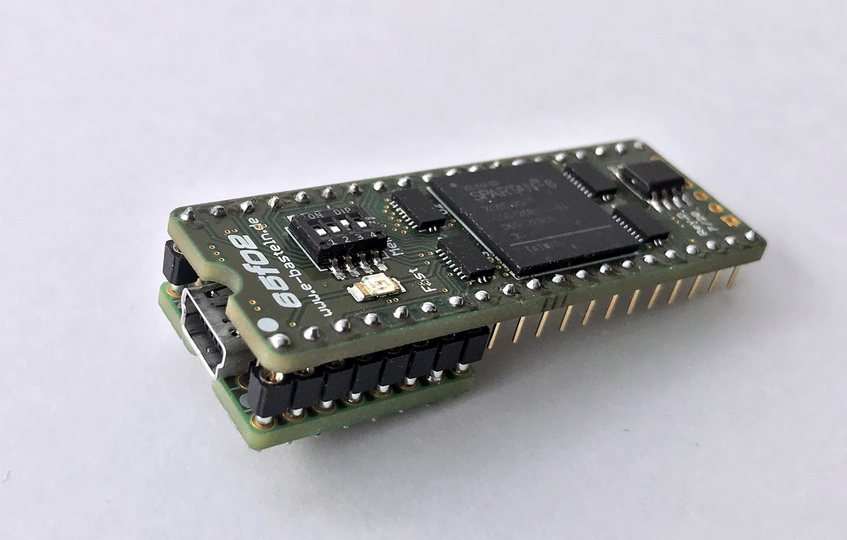
A simple, passive adapter board connects two unused pins on the DIP socket to the mini USB jack's data lines.
The Apple II can be expanded beyond 64 kByte of combined RAM and ROM by adding a “language card”, a 16 kByte memory expansion. Some late chess computers also have more than 64 kByte of addressable memory; mostly ROM in their case. To access this large memory despite the limited 64 kByte address space of the 6502, different blocks (“banks”) of memory are switched into the CPU’s address space via extra switching logic. This is controlled via access to a few reserved I/O addresses.
This is a headache for the 65F02. Since it grabs all RAM/ROM content at startup and then works from its internal RAM, it would remain completely unaware of the sudden change of memory contents. So the 65F02 needs to be taught about the host-specific memory switching scheme, and needs to essentially contain a copy of the host’s bank-switching logic. Even then, bank switching will mean performance compromises, because we only have 64 kByte of fast RAM available in the 65F02, so we can’t mirror and accelerate more than that amount of memory.
Not a very satisfying situation, but a compromise is better than no solution at all. And I do want to run UCSD Pascal fast on my Apple II! I have built support for the Apple II language card into the 65F02, and intend to add support for a couple of chess computers with large ROMs. (Hoping that the opening library can reside in slow host ROM, while the 65F02 mirrors the ROM areas which hold time-critical, recursive chess calculation routines.) But that’s probably the end of the line: More advanced memory management schemes, as used in the Apple //c or the BBC Master, are out of scope.
Some of the chess computers have battery backed-up RAM, so you can switch off the computer and continue your game the next day. But if all RAM lives on-chip inside the 65F02, nothing gets backed up unfortunately. In this case, the video RAM approach discussed above (routing every write access to both, the internal and external RAM) is not the right solution: Most RAM access is at the heart of the time-critical chess calculations, so it should be fast, rather than taking a full cycle of the slow host clock!
Instead, the 65F02 writes data back to battery-buffered host RAM in the background. A little state machine, separate from the CPU, reads byte for byte from the memory area that needs to be backed up. Since all RAM in the FPGA is dual-port memory, the state machine can get the data without getting in the way of the CPU. It then waits for a free bus cycle on the host bus (while the CPU is busy running from internal RAM), and uses that cycle to write the byte back to the host. With the typical 8 kByte RAM and 5 MHz clock rate of a decent 65C02-based chess computer, a full back-up cycle only takes 5 ms, assuming the bus is available one third of the time.
This feature is coded but still untested at this time (October 2020). Since I am running into routing congestions on the FPGA anyway, I might forfeit this to avoid adding more complexity in a timing-critical part of the design. And frankly, nobody has even asked for it anyway…